
Exhibition Hall Map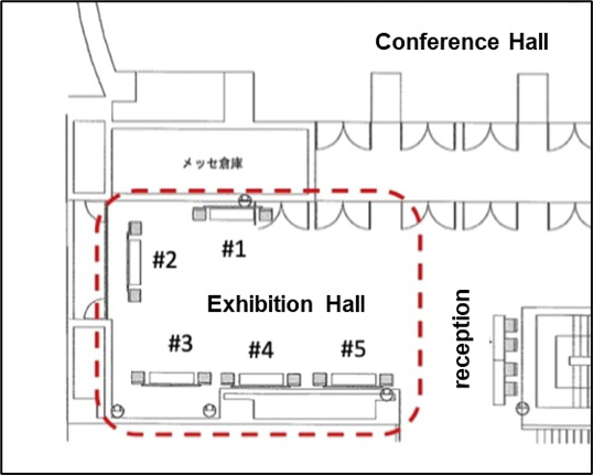
#1: TAKAYA, #2: Siemens EDA, #3: S.E.R., #4: Cadence, #5: FormFactor
Cadence Design Systems, Inc. (#4)
This booth will feature Cadence Modus DFT Software Solution that supports DFT/TEST design. Modus provides a complete set of industry-standard functions for memory BIST, logic BIST, test point insertion, and diagnostics reduce manufacturing test costs and increase silicon profitability. Modus is also integrated into Cadence Digital Full Flow, allowing for features such as 2D Elastic Compression and physical-aware test point insertion without impacting design size or routing.
FormFactor Inc. (#5)
FormFactor is a leading provider of essential test and measurement technologies along the full IC life cycle – from inspection and metrology, characterization, modeling, reliability, and design de-bug, to qualification and production test.
“From Lab to Fab”, Formfactor offers solutions for multiple phases of product development and delivery adding value along the design to test continuum .
Our product portfolio includes analytic probes, various types of probe cards, probing systems, 3D surface measurement systems and Quantum Cryogenics.
S.E.R Corporation (#3)
S.E.R. will exhibit unique spring probe and test socket products as follows.
- Super Short Probe
- 80GHz Coaxial test socket
- KTC series (Multi Channel Coaxial Cable Connector)
- mm wave interposer
- Multi-Impedance Solution
- Others
Siemens EDA (#2)
Siemens EDA is dedicated to helping companies engineer a smarter future faster by delivering the world’s most comprehensive portfolio of electronic design automation (EDA) software, hardware and services. At ITC Asia, Tessent showcases emerging adaptive intelligence solutions and features once-in-a-decade technology in Tessent Streaming Scan Network (SSN). SSN takes plug and play to the next level, reducing test time by 5x and cutting DFT development time in half. Tessent market-leading IC test solutions target the most critical defect mechanisms to improve quality and reliability across the silicon lifecycle and help accelerate yield ramp.
TAKAYA Corporation (#1)
Panel and Video presentation
- Flying Probe Tester
- In-circuit testing (ICT) is performed by moving multiple probes to some points on the board.
- No special jigs are required, and the settings can be changed simply by replacing the test program.
- Test point coordinates can be changed arbitrarily, making it easy to accommodate design changes.
- Flying Probe Tester and Boundary Scan Tester collaboration mutually
- Extended Coverage, Easier Analysis of Defective Locations, Reduce Costs
- Advantages of ODB++ to Create Test Programs
- Significantly Reduce the Time Required to Identify Defective Locations & Create Test Programs