Keynote 1 (Wednesday, Sept. 13)
Title: Semiconductor Packaging Revolution in the Era of Chiplets
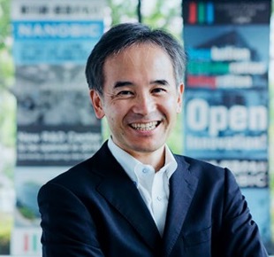
Speaker: Yasumitsu Orii (Rapidus Corporation)
Chair: Masahiro Ishida (ADVANTEST CORPORATION)
Abstract
Since the semiconductor cost for state-of-the-art nodes is increasing, “Chiplet” technology is in the spotlight as a new evolutionary path to scale up integration and improve performance and reduce the total cost. With an SoC, a chip might incorporate a CPU, plus an additional several IP blocks on the same chip. That design is then scaled by the advanced node, which is an expensive process. With a chiplet model, those several IP blocks are hardened into smaller dies(chiplets) and those dies are integrated on an interposer to build a system. Those chips must be connected in the shortest length while considering signal integrity and power integrity so that the cutting-edge packaging technology is the key to improve the performance of IT equipments. In this presentation, the advanced 2.1D, 2.3D, 2.5D and 3D packaging technologies will be introduced as well as the several interposer technologies.
About the Speaker
Dr. Yasumitsu Orii joined IBM Japan in 1986 and was a leading expert on Flip Chip organic packages, which had contributed to the performance improvements and miniaturization of such products as servers, laptop computers, and HDDs. The packaging technology is becoming more important for next generation server products as Moore’s Law reaches its limits. His flip chip expertise extended into many related areas. Initially, he was a pioneer of flip chip on FPC (Flexible Printed Circuit) for HDDs, which allowed the read/write amplifier ICs to be mounted on the suspension and much closer to the GMR head. Later, he developed the C2 (Chip Connection) technology that supported low-cost 50-μm-pitch flip chip bonding for the commodity consumer electronics market and it was licensed to a company in Taiwan. At IBM Research Tokyo, he was leading the next generation flip chip organic package, 3D-IC projects and Neuromorphic Computing for IBM Servers and creating new technologies under a Joint Development Program involving many leading Japanese materials companies. He left IBM in 2014 and joined NAGASE & CO., LTD. He established “New Value Creation Office” under the direct control of the president and launched the material informatics software as a service in 2020. He left NAGASE and he joined Rapidus Corporation in 2022/Dec. Now he is the senior managing executive officer to lead the 3D Assembly Division. He is IMAPS(International Microelectronics Assembly and Packaging Society) Fellow, IEEE EPS(Electronics Packaging Society) Senior member.
Keynote 2 (Thursday, Sept. 14)
Title: Technology for The Future of Computing
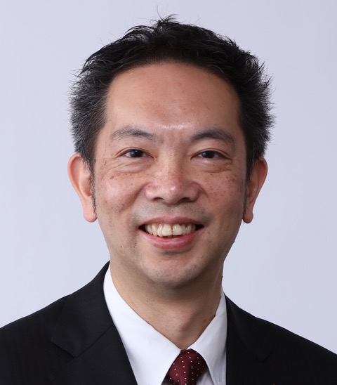
Speaker: Shintaro Yamamichi (IBM Japan, Ltd.)
Chair: Hideyuki Ichihara (Hiroshima City University)
Abstract
We are now facing a dramatical transformation in the IT industry, especially computing technologies. A new generation of the transistors, having a gate-all-around and nanosheet structure, is developed. In parallel, new semiconductor chips dedicated for the AI workload have been intensively studied. One technology, called Digital Core, can save the energy by reducing the precision in the calculation. The other technology, called Analog Core, utilizes non-volatile memory elements to represent the weights of the neural network in an analog way, and performs the multiply and accumulate operation by physical mechanism. Since it is quite difficult to implement all these technologies and architectures in one die, the advanced packaging technology, including testing methodology, will play a critical role in terms of system integration. Especially in a small form factor, such as in interposer substrate scale, the “chiplet” platform with both technology and design aspects should be developed, and recognized in the semiconductor ecosystem. Several chiplet technologies, such as micro bumping and Si bridge interconnect, will be introduced.
About the Speaker

Shintaro Yamamichi received his M.E. and Ph. D. degrees in electrical engineering, from Kyoto University, Japan in 1989 and 2002, respectively. He was involved in both semiconductor and packaging process research in NEC and Renesas Electronics. He was also a visiting industrial fellow at University of California, Berkeley in 1997. In 2013, he joined the Science and Technology team in IBM Research -Tokyo. From 2016, He led the research projects, including quantum computer installation, AI hardware, advanced packaging and material informatics. Currently, he is the Director of Semiconductors, IBM Research -Tokyo, leading all the semiconductor-related research and development activities in IBM Japan.


